10.1 inch 1024x600 TFT LCD Modules | UTF101C-CFN$
Model No. UTF101C-CFN$
- 10.1 inch TFT LCD
- Resolution : 1024x600 pixels
- View Direction: All
- Interface: LVDS
- IC:-
- Control-Board : No
- Brightness(typ.): 500 cd/m²
- Frame Through Hole: No
- Touch Screen : Without touch screen
數量
Description
Specification
Features
| Parameter | Dimension | Unit |
|---|---|---|
| Screen Size | 10.1 | inch |
| Display Resolution | 1024 x 3(RGB) x 600 | pixels |
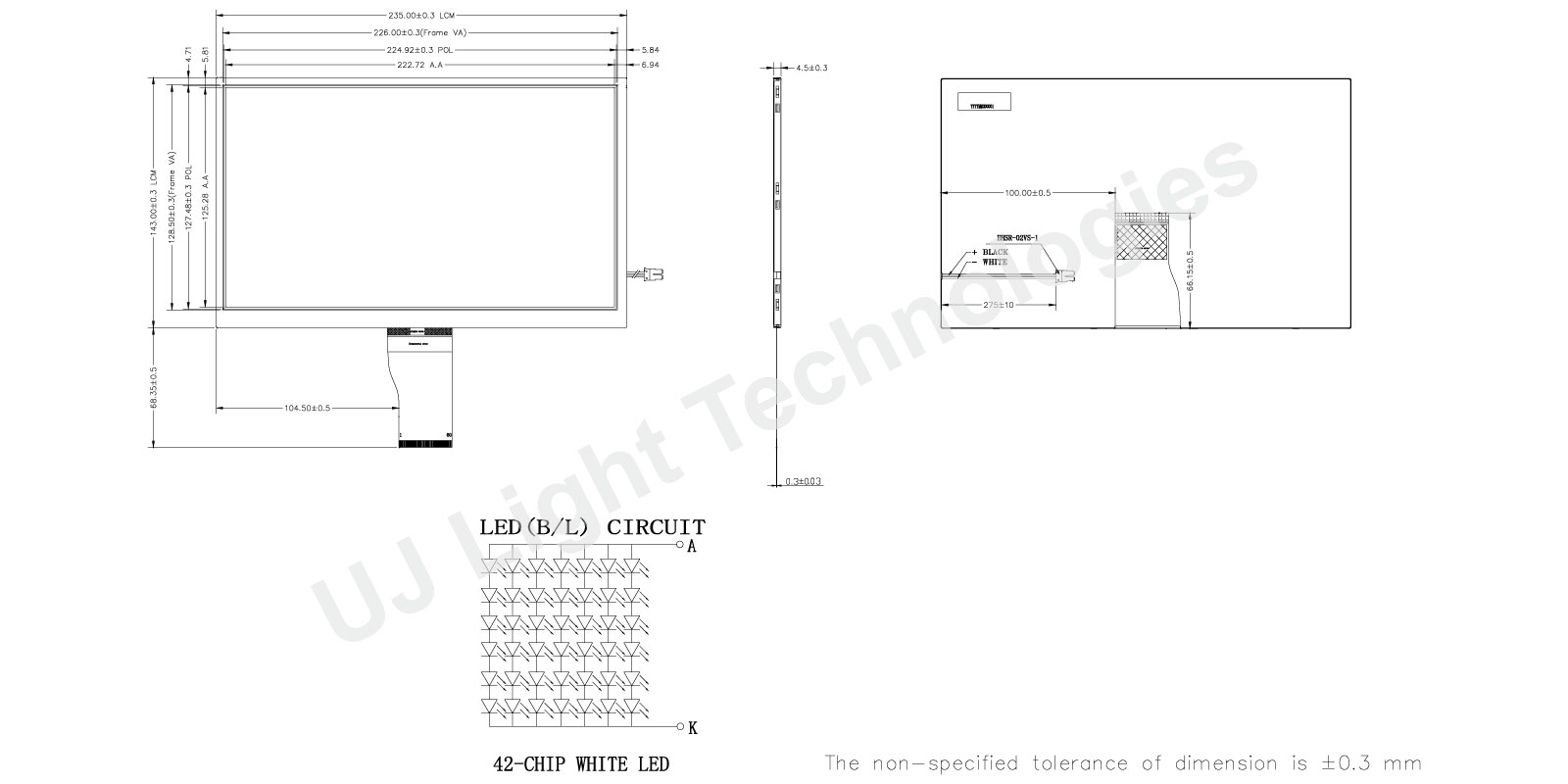
| Outline Dimension | 235.0(W) x 143.0(H) x 4.5(T) | mm |
| Active Area | 222.72(H) x 125.28(V) | mm |
| LCD Mode | a-Si TFT, Transmissive, Nomally white | |
| Driver IC | - | |
| Interface | LVDS | |
| View Direction | All | |
| Backlight Type | LED, Normally White | |
Absolute Maximum Ratings
| Item | Symbol | Min. | Typ. | Max. | Unit |
|---|---|---|---|---|---|
| Operating Temperature | TOP | -20 | - | +70 | ℃ |
| Storage Temperature | TST | -30 | - | +80 | ℃ |
Electrical Characteristics
TFT LCD Module (Ta=25±2°C)
| Item | Symbol | Min. | Typ. | Max. | Unit |
|---|---|---|---|---|---|
| Power Supply Voltage | VDD | 3.0 | 3.3 | 3.6 | V |
| Power Supply Voltage | AVDD | 7.0 | 9.6 | 13.5 | V |
| TFT Gate ON Voltage | VGH | - | 18 | - | V |
| TFT Gate OFF Voltage | VGL | - | -6.0 | - | V |
| Common Electrode Voltage | VCOM | - | 4.25 | - | V |
Backlight (Ta=25±2°C)
| Item | Symbol | Min. | Typ. | Max. | Unit |
|---|---|---|---|---|---|
| Supply Voltage | VF | 16.2 | 18.0 | 19.8 | V |
| Supply Current | IF | - | 140 | - | mA |
| Color | White | ||||
Interface
STBYB=0 TCON and source driver are off and all output are GND
| Pin | Symbol | Function |
|---|---|---|
| 1 | VCOM | Common Voltage |
| 2 | AVDD | Power For Analog Circuit |
| 3 | VDD | Power Supply Input Voltage |
| 4 | GND | Groud |
| 5 | VCOM | TFT Common Electrode Voltage |
| 6 | VDD | Power Supply Input Voltage |
| 7 | GND | Groud |
| 8~14 | V14~V8 | External gamma voltage pin floating |
| 15 | GND | Groud |
| 16 | VDD | Power Supply Input Voltage |
| 17 | GND | Ground |
| 18 | RXIN3+ | LVDS D3+ differential data input |
| 19 | RXIN3- | LVDS D3- differential data input |
| 20 | GND | Ground |
| 21 | RXCLKIN+ | LVDS CLK+ differential clock input |
| 22 | RXCLKIN+ | LVDS CLK- differential clock input |
| 23 | GND | Ground |
| 25 | RXIN2+ | LVDS D2+ differential data input |
| 25 | RXIN2- | LVDS D2- differential data input |
| 26 | GND | Ground |
| 27 | RXIN1+ | LVDS D1+ differential data input |
| 28 | RXIN1- | LVDS D1- differential data input |
| 29 | GND | Ground |
| 30 | RXIN0+ | LVDS D0+ differential data input |
| 31 | RXIN0- | LVDS D0- differential data input |
| 32~33 | GND | Ground |
| 34 | GRB | RESET Pin |
| 35 | STBYB | STBYB=1 All the functions are on(default) |
| 36 | SHLR | orizontal scan direction control pin |
| 37 | VDD | Power Supply Input Voltage |
| 38 | UPDN | Vertical scan direction control pin |
| 39 | GND | Ground |
| 40 | AVDD | Power For Analog Circuit |